Connector selection is often treated as a component-level decision. In a backplane or daughter-card assembly, it is a system-design decision. The connector determines how signals leave the board, how much routing area is available, how the board is supported mechanically, and how the assembly will be manufactured and serviced.
DIN 41612 Type C and card-edge connectors remain useful in applications where a repeatable board-to-board interface, accessible termination, and controlled mechanical arrangement are required. The correct choice depends less on connector name alone than on the relationship between contact arrangement, termination method, electrical allocation, PCB construction, and the complete mechanical stack-up.
The DIN 41612 Type C Three-Row Structure
DIN 41612 / IEC 60603-2 Type C connectors use three rows of contacts identified as rows a, b, and c. The contacts are arranged on 0.100-inch, or 2.54 mm, centers. This regular grid supports dense backplane and daughter-card interconnects while maintaining a predictable relationship between connector location and PCB geometry.
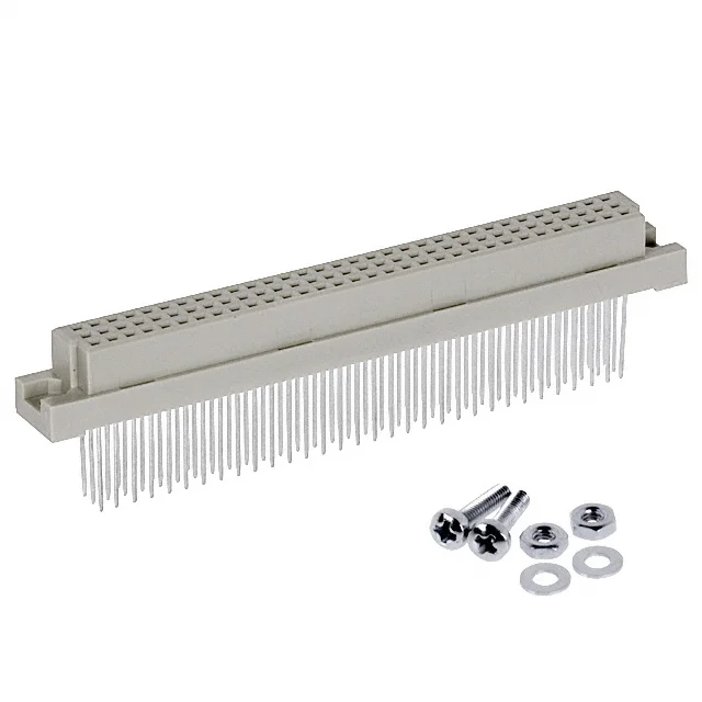
The row identifiers are positional references. They do not, by themselves, define whether a contact carries a signal, return, power, control, or another function. Those assignments are determined by the system architecture and the backplane schematic. A design should therefore document both the row and contact position rather than relying on a generic description such as “Type C connector.”
The best-known implementation is the 96-pin DIN connector used in VME backplanes. VME64x uses a five-row, 160-pin DIN connector that provides additional signal positions while retaining backward compatibility with traditional 96-pin DIN connectors. These applications illustrate why contact count alone is not a sufficient selection criterion. The row structure, pin assignment, mating arrangement, and board geometry must all remain consistent across the backplane and plug-in cards.
Contact density also affects signal integrity. As contacts become more closely grouped, the available escape area around the connector decreases. Routing must account for trace spacing, reference-plane continuity, via placement, power distribution, and the possibility of coupling between adjacent nets. A connector does not determine signal integrity by itself, but its contact density establishes constraints that the backplane layout must address.
Mating Considerations Between Backplane and Daughter Card
A typical backplane assembly places one connector half on the backplane and the mating half on the daughter card. The electrical interface may be standardized, but the physical implementation still requires careful definition.
The connector specification should identify:
- The mating connector type and orientation
- Male and female connector arrangement
- Row configuration and contact numbering
- Keying or polarization requirements
- Board-side termination method
- Tail geometry and available PCB area
- Card position relative to guides, rails, and adjacent boards
- Required clearance for insertion, extraction, inspection, and service
Mating compatibility should not be inferred from contact count alone. Two connectors may appear similar while differing in row arrangement, contact position, housing orientation, or termination geometry. The board footprint, schematic pin assignment, and mechanical drawings should be reviewed together.
Connector pitch is also a system-level constraint. Vector backplanes typically use a 4HP, or 0.800-inch, connector pitch. That spacing must be coordinated with card width, card guides, front panels, ejectors, adjacent components, and the available routing channel between connectors. A connector may fit the electrical interface and still create a mechanical interference if its housing, tail, or mating envelope is not included in the stack-up.
Wire-Wrap Versus Solder-Tail Terminations
Vector’s DIN 41612 / IEC 60603-2 Type C connectors are available with wire-wrap or solder-tail terminations. Both provide a valid connection method, but they support different manufacturing and service strategies.
| Termination | Primary design characteristic | Appropriate consideration |
|---|---|---|
| Wire-wrap | Accessible posts for wrapped wire connections | Useful where interconnects may be configured, modified, or probed during development and integration |
| Solder-tail | Board-mounted tails intended for soldered attachment | Appropriate where the connector is part of a fixed PCB assembly and the board process is defined |
Wire-wrap termination is valuable when the interconnect must remain accessible during prototyping, verification, troubleshooting, or configuration changes. It can simplify point-to-point changes without revising the PCB. However, the rear side of the connector requires sufficient clearance for the posts, wire routing, inspection, and any strain relief. The wire-wrap field must also be considered when the backplane is installed in a chassis or adjacent to another assembly.
Solder-tail termination provides a more integrated board assembly. It is generally selected when the connector location, PCB footprint, and circuit routing are fixed. The design must account for the tail pattern, plated-through-hole requirements, solder process, inspection access, and local thermal conditions. If reflow is part of the board assembly process, the connector construction and termination geometry must be confirmed as process-compatible rather than assumed to be compatible from the footprint alone.
Termination selection should be made before the backplane layout is released. Changing from wire-wrap to solder-tail, or the reverse, can alter the board outline, keep-out areas, rear clearance, assembly tooling, and inspection method.
How Connector Selection Drives Backplane Design
A backplane connector establishes a concentrated transition between the external board interface and the internal routing structure. This transition can influence layer count, trace topology, power distribution, and board stiffness.
Dense connector fields require disciplined breakout planning. Signal paths may need to change layers near the connector, while power and ground allocations may require broader copper structures. Maintaining an appropriate reference environment becomes more difficult when routing is forced through a small escape area. The result may be a need for additional PCB layers or a revised contact assignment that separates sensitive signals from higher-current or more aggressive nets.
Power distribution requires particular care. The number of available contacts is not the same as the usable power capacity of the connector. Current rating must be evaluated per pin and for the exact connector configuration, including temperature, contact allocation, parallel paths, PCB copper, and the intended operating environment. A backplane should not distribute power based only on the total number of contacts.
Mechanical design is equally important. Connector bodies and mating forces introduce localized loads into the PCB. A large backplane may require sufficient thickness, stiffening, mounting support, and controlled attachment points to prevent excessive deflection during mating. Card guides and chassis rails must keep the daughter card aligned with the connector so that the connector does not absorb unintended lateral or angular loads.
Vector backplanes use press-fit assembly throughout. That assembly approach must be incorporated into the PCB design, including the required hole pattern, board support, connector positioning, and installation tooling. In other assemblies, solder-tail connectors may be integrated with soldering operations. Press-fit and soldered attachment are not interchangeable late in the design process because they impose different board, process, and mechanical requirements.

Card-Edge Connectors for Daughter Cards and Prototyping
Card-edge connectors provide a different physical interface. Instead of using a separate connector half on the daughter card, the card exposes a defined edge interface that mates with the connector contacts. Vector card-edge connectors are available with dual rows of contacts in wire-wrap or solder-tail terminations.
The dual-row arrangement provides a compact interface for daughter cards, test boards, and prototype assemblies. As with DIN connectors, the card-edge contact assignment should be documented by position and row. The edge-finger geometry, board thickness, insertion alignment, and connector housing must be treated as one mechanical interface.
Wire-wrap card-edge connectors can be useful during development when the rear connection must remain accessible for changes or temporary wiring. Solder-tail versions are better suited to a fixed PCB assembly in which the connector is installed as part of the board manufacturing process.

Card-edge interfaces are also relevant to prototyping and troubleshooting. An extender board can move a circuit card away from the backplane while preserving the electrical interface, providing access to components and test points during development or fault isolation. The extender must maintain the same connector orientation and contact mapping as the target system; otherwise, physical access may be gained at the expense of interface accuracy.
Common Connector-Selection Mistakes
Several errors recur in backplane and daughter-card designs.
Confusing termination style with mating compatibility. Wire-wrap and solder-tail describe how a connector attaches to a board. They do not, by themselves, define whether two connector halves will mate. The mating interface, row arrangement, orientation, and contact geometry must be specified separately.
Ignoring current rating per pin. A connector with unused contacts is not automatically suitable for additional power distribution. Current must be allocated according to the exact contact rating and the thermal and PCB conditions surrounding it.
Underestimating the mechanical stack-up. The connector height, tail length, board thickness, card guide position, front-panel location, chassis clearance, and adjacent-board spacing must be checked as a complete assembly. A connector that is electrically correct can still fail to align with the card guide or create an interference at the rear of the backplane.
Treating contact density as only a packaging issue. Dense contacts affect breakout routing, reference planes, return-current paths, power allocation, and the resulting PCB construction. Signal-integrity analysis begins with the connector field and its pin assignment.
What Engineers and Program Teams Should Consider
Before releasing a connector definition, review the following items together:
- Is the interface based on DIN 41612 / IEC 60603-2 Type C or a dual-row card-edge connector?
- Which rows and contact positions are used, and how are they assigned electrically?
- Are the backplane and daughter-card connector halves correctly matched and oriented?
- Is wire-wrap or solder-tail termination appropriate for the intended assembly and service process?
- Does the termination require additional rear clearance, board support, or tooling access?
- Does the contact pitch fit the card guides, front panel, adjacent boards, and chassis?
- Has the backplane routing been evaluated for breakout area, reference planes, and signal coupling?
- Has current rating per pin been reviewed for power-distribution assignments?
- Does the PCB construction support the selected press-fit or soldered assembly method?
- Has the complete mechanical stack-up been checked before fabrication?
The connector should be treated as part of the backplane architecture, not as an isolated bill-of-materials entry. DIN 41612 Type C and card-edge families can support reliable daughter-card and backplane interfaces when contact mapping, termination, routing, assembly, and mechanics are defined as one controlled design.
Related Vector technical pages: DIN 41612 / IEC 60603-2 Type C Connectors, Card-Edge Connectors, VME J1/J2 Backplanes, and VME64/VME64x Backplanes.